UART programing in the TI ARM Tiva TM4C123G
The aim of the following exercise is to show how to make use of an UART port in the ARM Cortex-M4-based microcontroller Tiva TM4C123G LaunchPad. The ASIC character “Yes” will be send to a terminal emulator program on your PC as an example.

Resource: Tiva™ TM4C123GH6PM User Guide
The TM4C123G datasheet provide a series of steps under the below sections that will be required for UART set-up in the LaunchPad:
General-Purpose Input/Outputs (GPIOs) - Initialization and Configuration, page 649.
Universal Asynchronous Receivers/Transmitters (UARTs), page 893.
I will summarize those steps with a visual representation for a better understanding of the procedure and to easily go through the datasheet. Eventually each step will be part of an entire source code for you to use. Complete source code is at the end of this article.
Note: For the purpose of this tutorial, we are going to use IAR as our integrated development environment tool (IDE). I’m not affiliated, nor support, or receive any commission by doing so.
Note: Users should have been familiarized previously with the IAR tool.
To begin with...
You need to know that the Tiva ARM TM4C123GH6PM has up to 8 ports, designated as UART0 through UART7, for UART communication.
Table 23-5. GPIO Pins and Alternate Functions, page 1351 of the datasheet, shows all of the UARTs ports and correlation with their pins.

For simplicity, and because at the moment I don’t have any other cable other than the USB included in the box, we are going to program UART0. The reason why is because pins 17 & 18 of UART0 allow virtual COM connection between our device and the device driver at the host PC. And will work with communication software on the PC such as a terminal emulator.
%20and%20Port%201%20(Pin%2018)%20-%20COM.PNG)
Resource: Tiva™ TM4C123GH6PM User Guide, page 20.
In the TI LaunchPad, the pins 17 & 18 of the TM4C123GH6PM are connected to the ICDI (In-Circuit Debug Interface), which it turns out to be the USB connector. Thus, the USB cable would be suitable to communicate with UART0.
%20and%20Pin%2018%20(PA1).PNG)
From this point on the steps that you will follow represent single lines of code to be compiled later on in your source code. As mentioned before the complete source code can be found at the end.
Part I. GPIOA Initialization and Configuration
General-Purpose Input/Outputs (GPIOs) module, Port A.
DATA SHEET, p.656.
This section describes the steps to follow to access and configure the GPIO pins of a particular block. In our case the block we want to manipulate is block A, as we just see from the previous schematic pins 17 & 18 correspond to GPIOA.
STEP 1 - Enable the clock to the port by setting the appropriate bits in the RCGCGPIO register.
STEP 2 - Set the direction of the GPIO port pins by programming the GPIODIR register. A write of a 1 indicates output and a write of a 0 indicates input.
STEP 3A - Configure the GPIOAFSEL register to program each bit as a GPIO or alternate pin.
STEP 3B - If an alternate pin is chosen for a bit, then the PMCx field must be programmed in the GPIOPCTL register for the specific peripheral required.
STEP 4 - Set the drive strength for each of the pins through the GPIODR2R, GPIODR4R, and GPIODR8R
registers
STEP 5 - Program each pad in the port to have either pull-up, pull-down, or open drain functionality through
the GPIOPUR, GPIOPDR, GPIOODR register.
STEP 6 - To enable GPIO pins as digital I/Os, set the appropriate DEN bit in the GPIODEN register. To
enable GPIO pins to their analog function (if available), set the GPIOAMSEL bit in the
GPIOAMSEL register.
STEP 7 - Program the GPIOIS, GPIOIBE, GPIOEV, and GPIOIM registers to configure the type, event,
and mask of the interrupts for each port.
STEP 1. Enable signal clock to the appropriate GPIO module.
Datasheet - General-Purpose Input/Output Run Mode Clock Gating Control (RCGCGPIO), offset 0x608, p.340
Set the appropriate bits in the RCGCGPIO register to enable clock signal to the GPIOA.
,%20offset%200x608,%20p.340.PNG)
That is, set bit 0 in the RCGCGPIO to 1.
Code:
//Clock Gating Register
SYSCTL->RCGCGPIO |= 0x01; //STEP1: enable clock signal to GPIOA
STEP 2. Set the direction of the pins either as input or output.
SKIP STEP 2 - Not a feature needed at the moment.
STEP 3A. Enable the corresponding GPIO line with an alternate function.
Each GPIO line can be configured as a GPIO or have another alternate function.
Table 23-5 on page 1351 details which functions are mixed on each GPIO pin.

As can be seen from the above table, there are two different functions for, PA0 and PA1. This means that "ALT function" needs to be enabled in the GPIOAFSEL, since both can act as either UART or CAN.
Datasheet - GPIO Alternate Function Select (GPIOAFSEL), offset 0x420, p.671.
,%20offset%200x420,%20p.671.PNG)
Note: We set bits 1-0 because those represent pins 17 & 18. PA0 = 17, PA1 = 18. See the schematic.
STEP 3B. Selects the specific peripheral signal for the corresponding selected GPIO line.
Datasheet - GPIO Port Control (GPIOPCTL), offset 0x52C, p.688
Each PMCn field in the GPIOPCTL register represents a GPIO line. 8 lines in total -> from bit 0 to 31.
%20-%20PMCn.PNG)
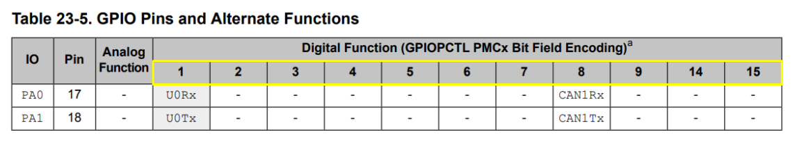
Digital Function 1 is the value that should be placed in the PMC0 and PMC1 fields of the GPIOPCTL register to assign the UART ALT function to the GPIO Port A line PA0 (Rx) and PA1 (Tx).
Code:
GPIOA->PCTL = 0x11; /* STEP3B. Configure PA0 and PA1 for UART */
STEP 4. Set the drive strength for each of the pins through the GPIODR2R, GPIODR4R, and GPIODR8R registers.
.PNG)
Enable GPIODEN register bits 1:0 as digital by setting bits from 0 to 1 to one.
GPIOA->DEN = 0x03; /* STEP6. Enable PORTF2-0 DIGITAL pins */
STEP 7: Enable and configure the GPIO Interrupt options
SKIP STEP 7 - Not a feature needed at the moment.
Part II. UART Initialization and Configuration
Datasheet - Universal Asynchronous Receiver/Transmitter Run Mode Clock
Gating Control (RCGCUART), offset 0x618, p.344STEP 2. Disable UART0 before making any changes.
Disable the UART by clearing the UARTEN bit in the UARTCTL register.
Datasheet - UART Control (UARTCTL), offset 0x030, p.918
.PNG)
3A. Write the integer portion of the BRD to the UARTIBRD register.
.PNG)
UART0->IBRD = 104; /* STEP3A. 16Mhz/16 = 1MHz, 1Mhz/104 = 9600 baud rate */
3B. Write the fractional portion of the BRD to the UARTFBRD register.
Datasheet - UART Fractional Baud-Rate Divisor (UARTFBRD), offset 0x028, p.915
.PNG)
Code:
UART0->FBRD = 11; /* STEP3A. fraction part, see Example 4-4 */
STEP4. Write the desired serial parameters to the UARTLCRH register (in this case, a value of 0x0000.0060).
Desired UART Serial configuration:
¦ 9600 baud rate
¦ Data length of 8 bits
¦ One stop bit
¦ No parity
¦ FIFOs disabled
¦ No interrupts
Datasheet - UART Line Control (UARTLCRH), offset 0x02C, p.916
Code:
UART->LCRH = 0x60; /* 8-bit, no parity, 1-stop bit, no FIFO */
.PNG)
STEP6. Optional
%20-%20TEN.PNG)
Part III. UART Flag Register (Status)
void UART0Tx(char c)
{
/* -------------------------- PART III -------------------------- */
while ((UART0->FR & 0x20) != 0);/* wait until Tx buffer not full */
UART0->DR = c; /* before giving it another byte */
/* ----------------------- PART III (END) ----------------------- */
}
- You Initialize and Configure the GPIO Port A and the UART module.
- Plus set up the status flag for monitoring to know when to send the character “Yes” to the terminal emulator program at your PC.
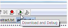
Press the Download & Debug at the top of the IAR tool bar to upload the code to your Tiva LaunchPad.
Resource: Boost your daily development cycle!
Then, open your terminal emulator program (PuTTY for example). Serial configuration is as follows: Note: Go to Device Manager and validate which COMX is your Tiva LaunchPad connected to.

- Open a section. You should be able to see the word “Yes” in the terminal emulator screen.

CODE:
1 2 3 4 5 6 7 8 9 10 11 12 13 14 15 16 17 18 19 20 21 22 23 24 25 26 27 28 29 30 31 32 33 34 35 36 37 38 39 40 41 42 43 44 45 46 47 48 49 50 51 52 53 54 55 56 57 58 59 60 61 62 63 64 65 66 67 68 69 70 71 72 73 74 75 76 77 78 79 80 81 82 83 84 85 86 87 88 | /* UART Sending "Yes" to UART0 on TI ARM Launchpad (TM4C123GH6PM) UART0 is on USB/Debug Use PuTTY to see the message "YES" on a PC Desired UART configuration: ¦ 9600 baud rate ¦ Data length of 8 bits ¦ One stop bit ¦ No parity ¦ FIFOs disabled ¦ No interrupts */ #include <stdint.h> #include <TM4C123GH6PM.h> //Tiva C Series TM4C123G “Header File”. void GPIO_init(void); void UART0_init(void); void UART0Tx(char c); void delayMs(int n); int main(void) { GPIO_init(); UART0_init(); delayMs(1); /* wait for output line to stabilize */ for (;;) { UART0Tx('Y'); UART0Tx('E'); UART0Tx('S'); UART0Tx(' '); } } void GPIO_init(void) { /* ---------------------------- PART I ---------------------------- */ /* ------------ GPIOA Initialization and Configuration ------------ */ SYSCTL->RCGCGPIO |= 0x01; /* STEP1. Enable clock signal to the GPIOA */ /*SKIP STEP2*/ GPIOA->AFSEL = 0x03; /* STEP3A. Use PA0, PA1 alternate function */ GPIOA->PCTL = 0x11; /* STEP3B. Configure PA0 and PA1 for UART */ /*SKIP STEP4 - 5*/ GPIOA->DEN = 0x03; /* STEP6. Enable PORTF2-0 DIGITAL pins */ /* ------------------------ PART I (END) -------------------------- */ } void UART0_init(void) { /* --------------------------- PART II -------------------------- */ /* ----------- UART Initialization and Configuration ---------- */ SYSCTL->RCGCUART |= 1; /* STEP1. Enable clock signal to UART0. */ UART0->CTL = 0x00; /* STEP2. Disable UART0 before any changes */ /* desire configuration */ UART0->IBRD = 104; /* STEP3A. 16Mhz/16 = 1MHz, 1Mhz/104 = 9600 baud rate */ UART0->FBRD = 11; /* STEP3B. Fraction part, see Example 4-4 */ UART0->LCRH = 0x60; /* STEP4. 8-bit, no parity, 1-stop bit, no FIFO */ UART0->CC = 0; /* STEP5. Use system clock */ /*SKIP STEP6*/ UART0->CTL = 0x301; /* STEP7. Enable UART0, TXE, RXE */ /* ------------------------ PART II (END) ------------------------ */ } void UART0Tx(char c) { /* --------------------------- PART III -------------------------- */ /* ----------------- UART Flag Register (Status) ----------------- */ while ((UART0->FR & 0x20) != 0); /* wait until Tx buffer not full */ UART0->DR = c; /* before giving it another byte */ /* ------------------------ PART III (END) ----------------------- */ } void delayMs(int n) { int i, j; for(i = 0; i < n; i++) for(j=0; j < 3180; j++) {} // do nothing for 1 ms } |
Comments